PhD Thesis
(2009-2014)
Micro-Electro-Discharge Machining of Carbon-Nanotube Forests and Its Application
THE UNIVERSITY OF BRITISH COLUMBIA
(Vancouver, Canada)
Carbon nanotubes (CNTs) are relatively new materials with exceptional properties which have attracted significant interest in the past two decades. The ability to grow arrays of vertically aligned carbon nanotubes, so called CNT forest, opened up opportunities to develop different types of novel devices enabled by the material. A key in facilitating micro-electro-mechanical systems (MEMS) applications of the material is the ability to pattern the material in a batch mode with high precision and high reproducibility. Patterning CNT forests prior to, during or after the growth is reported. The mentioned techniques are, however, primarily for the formation of two-dimensional types of patterns (with uniform heights). Laser micromachining is reported to shape CNT forests for different applications while exhibiting its inherent limitations including tapered sidewalls, lack of high-precision depth control, and thermal damages. Hence, there is a need to develop machining techniques to fabricate CNT forests in any shape for MEMS and other applications.
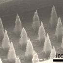
This thesis is based on the idea that a powerful micromachining technique is a path that should be taken to reach a successful integration of smart materials such as nanotubes and MEMS (and other) devices to achieve more complex and improved devices. This work develops a powerful micromachining technique based on dry micro-electro-discharge machining (µEDM) to produce free-form, three-dimensional (3D) patterns out of CNT forests with high precision (~2-µm machining tolerance and spark size of few hundred nanometers), high-aspect-ratios (of about 20), high reproducibility, and at very small machining voltages (~10 V). We found out the machining mechanism is different from the one in typical µEDM. Techniques to achieve higher-resolution removal precision are investigated. Elemental and molecular analyses of the machined structures are carried out to observe the level of cross-contamination of the process. To demonstrate few applications of the processed nanotubes, we focused on developing high-power MEMS switches integrating micropatterned CNT forests as electrical contact. Micropatterned CNT forests as field emitters and atomic force microscopy (AFM) probe tips are also demonstrated.